

China Light Guide Plate Innovations You Should Know for Better Display Performance
2026-11-16
Displays only look as good as the light behind them allows. In the quest for brighter, thinner, and more uniform screens, light guide plate technology has quietly become a deciding factor. From edge-lit panels to high-transmission acrylic designs, small changes in plate structure can dramatically shift brightness, color consistency, and viewing angles. If you're evaluating display performance, ignoring these innovations means accepting avoidable compromises. This guide breaks down the China light guide plate advances that are reshaping visual output—and shows how Meld Display is turning those advances into measurable gains for real-world applications.
Dotless micro-lens textures that smooth out edge-lit panels
Edge-lit panels often struggle with visible LEDs and abrupt falloff near the frame. A dotless micro-lens texture replaces the familiar dot pattern with a continuous arrangement of microscopic refractive shapes, letting the surface distribute light without revealing its structure. The result is a panel that reads as a single, even wash instead of a field of bright points.
Because the lenses are formed directly into the light guide during tooling, the diffusion happens at the source rather than through an added diffuser sheet. This keeps the stack thinner and reduces the soft haze that heavier films can introduce. Tight control over lens depth and pitch smooths the transition from the injection edge to the center, so corners and long edges stay consistent even on larger panels.
The visual quietness also matters in finished fixtures. Without visible dot stepping or mura, the panel supports lower-profile bezels and cleaner industrial design, while still meeting uniformity targets in slim luminaires.
Why thinner light guide plates demand shorter LED coupling gaps
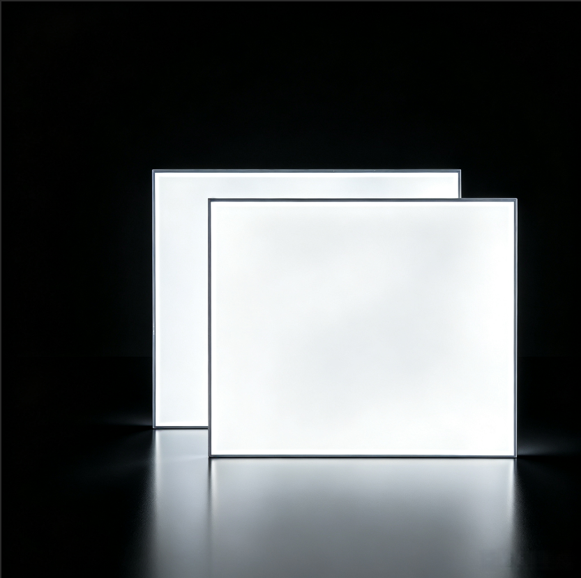
As light guide plates become thinner, the edge face available for LED light injection shrinks considerably. A typical LED package aperture often exceeds the plate thickness, so some emitted flux strikes the top or bottom surface near the entry edge instead of entering cleanly through the edge. Reducing the lateral gap does more than capture extra rays; it changes how much of the LED’s near-lambertian output actually overlaps the narrow input aperture.
With a thicker plate, a modest gap still allows the light cone to expand and fill the guide without obvious hot spots. A thin plate, however, has a very narrow acceptance angle at the edge. If the LED sits too far back, high-angle rays arrive at the entry plane already spread beyond the plate thickness, reflecting off the front surface or creating bright bands just inside the active area. Moving the LED closer keeps the more divergent portion of the beam within the plate’s numerical aperture.
There is also a mechanical alignment factor. In thin designs, any lateral offset or gap variation produces a larger relative change in coupling efficiency because the margin for error is smaller. A shorter coupling gap reduces the effect of LED placement tolerance and gives the light more chance to enter before it can spill into the bezel. The practical result is better initial mixing and fewer visible artifacts near the injection edge.
V-cut angle shifts that erase bright bands near the light source
Near the light entry edge, bright bands often appear because the first extraction features receive a concentrated burst of light before the flux spreads evenly through the guide plate. A static V-cut angle makes this worse by pulling too much light out in the first few millimeters. Shifting the cut angle in that zone lowers the extraction efficiency just enough to hold more light in the plate, letting it travel farther before it escapes.
The shift is rarely uniform. Angles can be steepened or shallowed in a gradual pattern, or the groove asymmetry can be altered so the facet that faces the LED reflects less light upward at close range. This creates a smoother transition from the injection area to the middle of the panel. Matching the angle progression to the LED pitch, refractive index, and plate thickness is what makes the bright band disappear without adding visible dark patches.
In production, the adjustment often appears as a localized V-cut angle offset rather than a complete redesign of the pattern. Even a small angular change near the light source can redistribute enough energy to remove the visible hot spot. The result is cleaner edge-to-edge uniformity, especially in slim panels where the mixing distance is limited.
High-purity PMMA grades with lower haze for sharper handheld screens
The push toward brighter, more pixel-dense handheld displays has exposed a quiet bottleneck: the light-transmitting layers sitting between the LED array and the user's eyes. High-purity PMMA grades are now being refined with tighter control over residual monomer and microscopic gel particles, two factors that rarely show up on standard datasheets but directly influence how light scatters as it passes through the sheet. By reducing these internal imperfections, manufacturers achieve lower haze values without sacrificing the mechanical toughness that makes PMMA preferable to glass in drop-prone devices.
Lower haze translates into something very practical on a handheld screen: crispness that survives real-world viewing angles. When haze drops from 1.5% to under 0.6%, edge contrast improves noticeably, and small text or UI icons no longer appear to bleed into a faint glow. This matters most in sunlight, where scattered light otherwise washes out black levels and forces higher backlight power. High-purity grades also exhibit better color neutrality across the visible spectrum, so the panel's calibration holds steady instead of drifting toward a slight warm or cool cast over time.
For display stack engineers, the benefit is as much about process stability as optical performance. These PMMA grades flow more predictably during extrusion and injection molding, reducing the incidence of flow lines or microvoids that act as secondary scattering centers. The result is a cover lens or light guide plate that meets tighter haze specifications without adding post-processing steps. As handheld devices continue to shrink bezels and push peak brightness, specifying the right PMMA purity level becomes one of the quieter levers for delivering the sharpness consumers now expect from even mid-range phones.
Tapered plate designs that drop weight without dimming the corners
Rather than removing material evenly across the whole surface, a tapered plate keeps the corners thicker while the middle section becomes noticeably leaner. The transition is the part that takes real work: if the taper starts too soon, the edges lose rigidity; if it starts too late, the weight savings barely register. Done carefully, the plate still feels planted at every corner without carrying unnecessary mass through the center.
That balance changes how a board sounds and handles. The reduced center weight gives a slightly more open, less dead response, yet the corners stay firm enough to keep switch alignment stable and the assembly from flexing when it is picked up by one side. It is a subtle difference, but once you compare a straight cutout plate with a well-tapered one, the uneven stiffness becomes easy to notice.
Producing this shape is more demanding than adding slots or drilled holes. The taper needs to follow the structure rather than fight it, and even small errors in thickness can introduce warping or weak spots near the edges. When the machining is dialed in, the plate looks almost stock from a distance, but the drop in weight is immediate the moment it reaches your hands.
Thermal cycling tests that separate warp-resistant plates from the rest
Thermal cycling tests don’t reward optimistic material choices. A plate can look perfectly flat on the bench, yet after exposure to repeated swings between -40°C and 125°C, residual stress finds a way out. The first signs usually appear near mounting holes or machined edges, where a slight ripple becomes a measurable bow. Warp-resistant grades tend to move less than 0.2 mm across a 300 mm span even after 200 cycles, while ordinary plates drift past that threshold long before the test concludes.
The distinguishing factor often isn’t stiffness alone. Resin systems with lower moisture absorption and a glass transition comfortably above the upper soak temperature hold their shape because they don’t soften during the hot phase. Fiber architecture matters too: balanced laminates with symmetric layups avoid the internal tug-of-war that shows up as corner lifting. In practice, this means the plates that pass are the ones where thermal expansion is managed layer by layer rather than corrected afterward.
What makes the test useful is its honesty. A plate that survives slow, uniform heating in an oven may still fail under rapid air-to-air cycling because transient gradients create temporary stress concentrations. By the time a warp-resistant plate emerges, it has accumulated small elastic recoveries without crossing into permanent set. The failures, by contrast, reveal themselves early and without ambiguity.
FAQ
The industry has largely shifted from printed dots to micro-scale optical structures created by laser etching, UV imprinting, or hot embossing. Those structures can be shaped as rounded cones, tapered ridges, or lens-like bumps, which direct light more efficiently and allow thinner plates without the usual uniformity penalty.
Curved, high-brightness cockpit screens need light management that stays consistent across wide temperature swings and direct sunlight. Chinese suppliers have responded with low-birefringence materials, tighter pattern tolerances, and custom contrast-enhancing surface finishes, which help the backlight remain readable without pushing LED power too high.
Rather than relying on a uniform dot pattern, they adjust the local density, depth, or shape of micro-patterns according to the distance from the LEDs. Simulation tools map out the irradiance first, then the manufacturing line reproduces that variable pattern precisely. This keeps the area near the light source from looking brighter than the center.
Large TVs get a lot of attention, but the same technologies also improve tablets, monitors, and industrial displays. Thin plates with high uniformity are especially useful in portable and battery-powered devices, where every bit of optical efficiency reduces the number of LEDs and extends battery life.
Continuous roll-to-roll hot embossing and high-speed laser direct writing are two notable examples. They allow fine features to be reproduced over wide formats with less drift, while automated optical inspection catches defects before sheets are cut or shipped. This combination of precision and throughput is hard to match with older screen-printing methods.
It determines how light is distributed across the plate before production starts. A well-tuned design accounts for LED spacing, plate thickness, film stack, and reflector placement, then generates a pattern that keeps luminance variation low. Suppliers that develop or customize this software internally can typically adapt faster when a new backlight layout appears.
Request uniform luminance maps captured at the final thickness and with the intended optical films, because a bare plate can look better than a fully assembled backlight. Also ask about tolerances for pattern depth and repeatability across the sheet, since those factors decide whether the first article matches volume production.
Conclusion
Chinese light guide plate makers have moved well beyond conventional printed dot patterns. The shift to dotless micro-lens textures is now common in edge-lit panels, where carefully tuned lens arrays smooth out the uneven glow that older designs often produced near the middle of the screen. At the same time, thinner plates are forcing backlight teams to rethink LED coupling. A shorter gap between the LED and the plate edge reduces light leakage and keeps efficiency from dropping as the panel gets slimmer. V-cut angle adjustments have also become a practical fix for the bright bands that frequently appear close to the light source, with revised groove angles scattering light more evenly before it travels across the viewing area.
Material and structural changes matter just as much. High-purity PMMA grades with lower haze are giving handheld displays cleaner contrast and sharper text, especially under bright ambient light. For larger or portable formats, tapered plate designs are being used to cut weight without letting the corners fall into shadow, balancing thickness transitions carefully across the full surface. Perhaps the quietest but most telling advance is in validation. Thermal cycling tests now separate warp-resistant plates from cheaper options that look fine at room temperature but deform after repeated heating and cooling. Together these improvements point to a supply base that is competing less on raw price and more on optical consistency and long-term reliability.
Contact Us
Contact Person: Sky Wang
Email: [email protected]
Tel/WhatsApp: 8613430620125
Website: https://www.meldled.com/