Considerations related to double-sided boards
2023-11-15
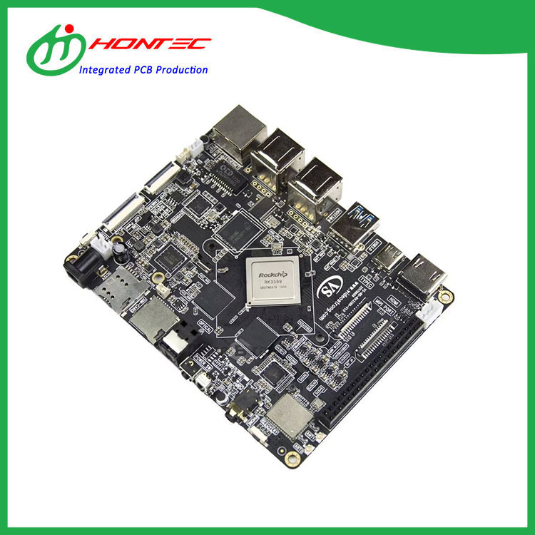
A double-sided board, also known as a double-sided PCB (Printed Circuit Board), is a type of circuit board that has conducting layers on both sides of the board. In contrast to single-sided boards that have conductive traces on only one side, double-sided boards provide more routing space and increased flexibility in the placement of components.
Here are key features and considerations related to double-sided boards:
1. Two Conductive Layers:
- A double-sided board has a conductive layer on both the top and bottom surfaces. These layers are typically made of copper, and they are etched or printed to form the required circuitry.
2. Via Holes:
- To establish electrical connections between the top and bottom layers, via holes are used. These are holes drilled through the board and then plated with conductive material to create a pathway for signals or power to pass between layers.
3. Increased Component Density:
- With two conductive layers, designers have more freedom to route traces and place components, allowing for higher component density compared to single-sided boards.
4. Improved Signal Integrity:
- Double-sided boards can be advantageous for circuits that require enhanced signal integrity or have more complex routing needs, as the two layers provide additional routing options.
5. Applications:
- Double-sided boards are widely used in various electronic devices, ranging from consumer electronics to industrial applications. They are versatile and cost-effective for many designs.
6. Surface Mount and Through-Hole Components:
- Double-sided boards can accommodate both surface-mount and through-hole components, providing flexibility in component selection.
7. Cost-Effective:
- While not as complex or costly as multi-layer boards, double-sided boards strike a balance between complexity and cost. They are often a cost-effective solution for many applications.
8. Prototyping:
- Double-sided boards are commonly used in prototyping due to their flexibility and ease of design modifications.
9. Assembly Process:
- The assembly process for double-sided boards involves placing and soldering components on both sides of the board. Special care is taken during the soldering process to avoid damaging components on the opposite side.
10. Design Challenges:
- Routing signals and power across layers can present challenges, and designers need to carefully plan the placement of vias to optimize signal integrity and avoid interference.
Double-sided boards are a popular and widely used choice in electronics design due to their versatility, cost-effectiveness, and suitability for a broad range of applications. However, for more complex designs with higher-density requirements or specific performance criteria, designers may opt for multi-layer boards with additional internal conducting layers.


